
技术
Page 2 of 4
One of the best techniques to characterise the microstructure of a sample is electron backscatter diffraction (EBSD). EBSD is a technique in the scanning electron microscope (SEM): a flat and polished, crystalline sample is positioned in the SEM sample chamber at a high tilt from the horizontal (usually 70°) and the electron beam is focussed into a spot on the surface. The incident electrons interact with the atoms close to the surface of the sample (typically the top 10-200 nm) and are scattered in many directions, losing just a small fraction of their energy. Some of these scattered electrons will impinge upon the planes of atoms in the crystal lattice in such a way that the conditions for Bragg diffraction are satisfied:
nλ = 2dsinθ
Where n is an integer, λ is the wavelength of the electrons (which in turn is inversely related to the electron beam energy or accelerating voltage), d is the spacing of the lattice plane in question and θ is the angle of incidence. If we place a fluorescent phosphor screen close to the sample, these diffracted electrons will form pairs of curved lines for each lattice plane. These are known as “Kikuchi” lines and the bands that they form “Kikuchi bands” (named after the Japanese physicist, Seishi Kikuchi). There are many lattice planes in a crystal, and therefore the resulting “diffraction pattern” is made up of multiple overlapping Kikuchi bands, with a distinct appearance. The diffraction pattern generated using the EBSD technique is usually referred to as an electron backscatter diffraction pattern (EBSP).
A typical geometry for EBSD, showing the tilted sample and the EBSP projected onto a phosphor screen at the end of the EBSD detector
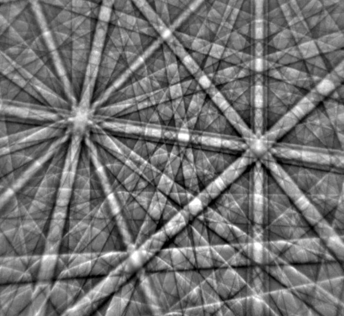
A typical high-quality EBSP, with multiple overlapping Kikuchi bands
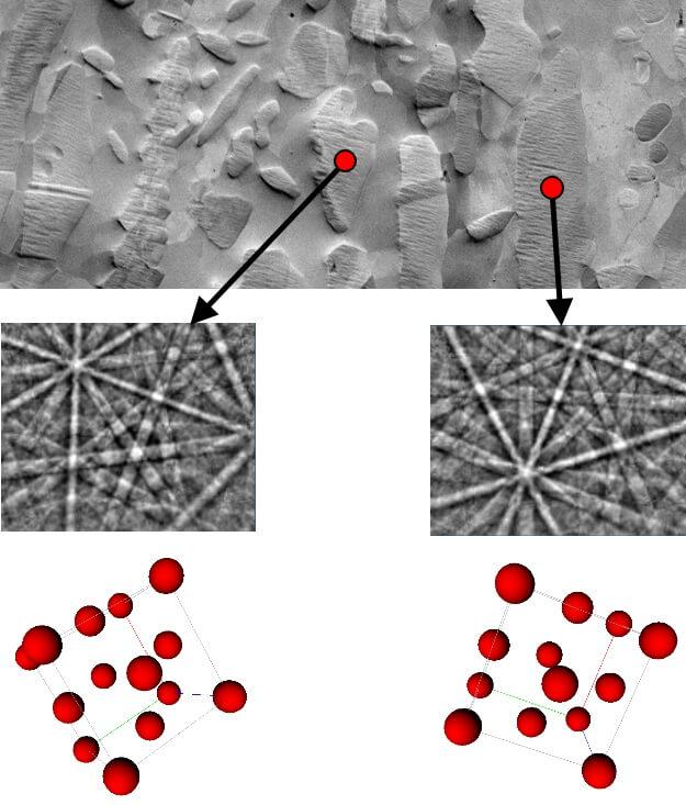
The symmetry and appearance of the pattern is related intimately to the crystal structure at the point where the beam meets the sample. If the crystal rotates (in other words its orientation changes) the diffraction pattern will be seen to move. If a different type of material (a different “phase”) is placed under the beam, the diffraction pattern will change completely. So, if we know enough about the atomic structure of the phases that are in our sample, the diffraction pattern can be used to measure crystal orientations and to identify and differentiate between phases.
Image example showing the relationship between the EBSP and the atomic lattice orientation for different grains in a stainless steel sample. The top image is scanning electron micrograph showing the different grains in the steel. The diffraction pattern and crystal orientation are shown for 2 grains of austenite (face centred cubic Fe) marked by the red circles.
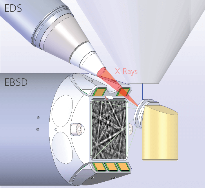
Usually the process of analysing and indexing the diffraction pattern is fully automated using dedicated software. This process can be extremely fast, with modern systems capable of collecting and indexing the diffraction patterns at rates of many 1000s per second. This speed, coupled with the technique’s high spatial resolution (10s nm on most materials) and the high precision of orientation measurements (0.1-1°), make EBSD a very powerful technique. In addition, most commercial EBSD systems can be integrated with energy dispersive X-ray spectrometry (EDS) - a technique that measures sample composition - thus providing a comprehensive analysis of both crystallography and composition.
A technique that measure sample composition - thus providing a comprehensive analysis of both crystallography and composition. Taken together, this is an ideal combination for characterising microstructures.
© 牛津仪器 2026
 公安机关备案号31010402003473