半导体、微电子和存储器

EBSD技术,以及拥有着更高分辨率的TKD技术,在半导体和微电子工业中有诸多不同的应用。许多材料的电性能与它们的微观组织,特别是晶粒尺寸、织构和界面性能,有着内在的联系。仅凭EBSD或TKD分析,就可以提供所有需要的信息,其分辨率适合除最细微的纳米结构外的所有的纳米结构。也许,在这领域里,最常见的应用是在电子封装,例如:焊锡凸块或引线键合的表征。EBSD还可用于测量薄膜中位错的密度和类型(例如,用于发电和发光二极管应用的II-VI族半导体中的线位错),或提高我们对存储设备中的纳米结构的理解。EBSD和TKD在这个领域的应用案例包括:

焊锡凸块的EBSD分析
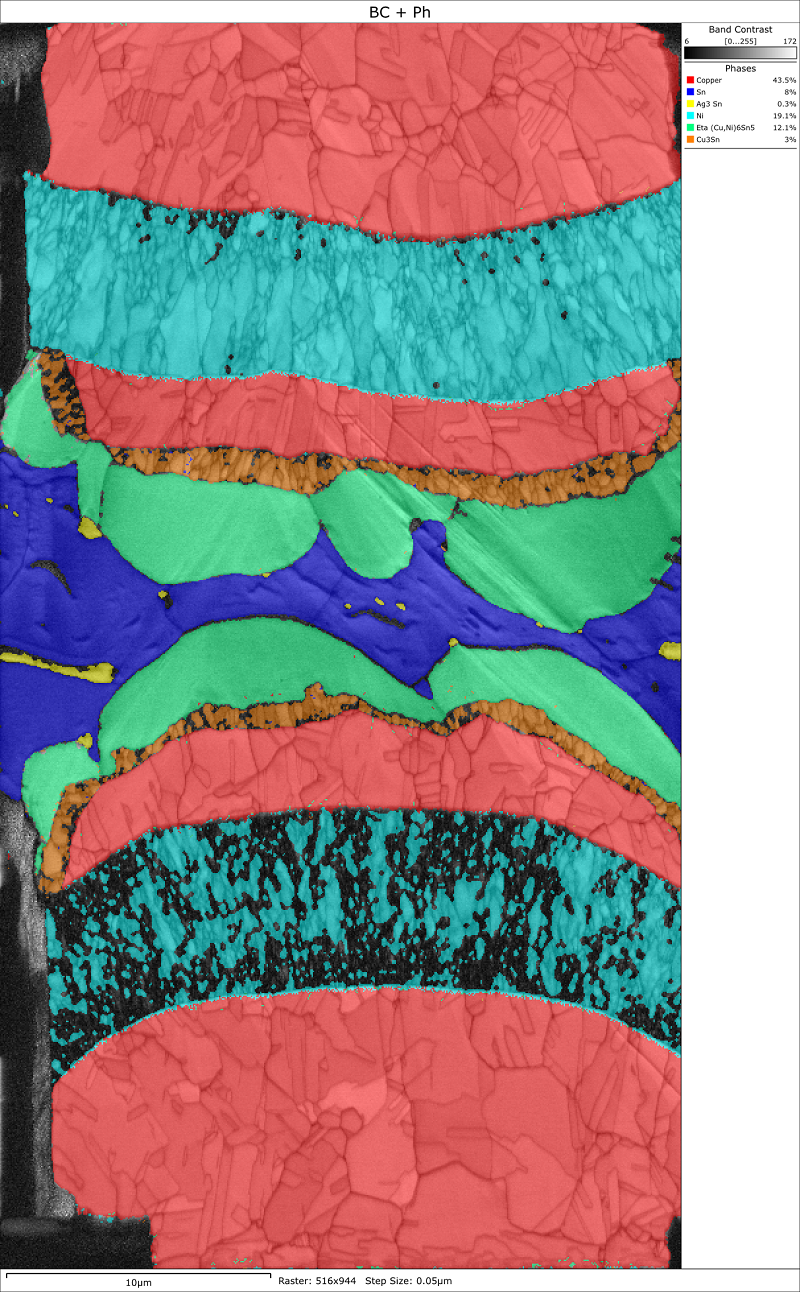
EBSD相分布图显示无铅微凸点中复杂的相分布
相分布图(Cu—红色,Sn—深蓝,Ni—浅蓝,Ag3Sn—黄色,Cu3Sn—橙色,η-Cu6Sn5—绿色
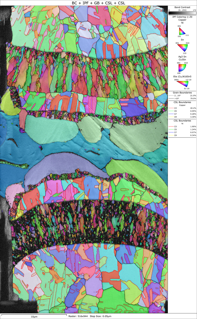
EBSD取向图显示了无铅微凸点的不同层内的复杂结构
取向图(IPF-Z着色方案),突出Cu和Ni的重合点阵(CSL)晶界。

Application Notes

EBSD Applications in the Electronics Industry

This application note provides several brief examples of the use of the EBSD technique and, in particular, the Symmetry S2 detector and the AZtecCrystal data processing software, for the effective characterisation of microstructures in a range of microelectronics samples.

了解更多
Applying nanomanipulation to the EBSD analysis of a gold wire

This application note describes a method of combining Oxford Instrument’s OmniProbe tools and AZtec EBSD system for the manipulation and analysis of a 5μm diameter gold microelectronic wire sample.

了解更多

Webinars

Semiconductor failure analysis solutions 

Semiconductor failure analysis requires painstaking detective work to understand the source of failures so that they can be removed from volume production. Discover how Oxford Instruments solutions can enable you to overcome these and other challenges.

Watch on demand
Nano-characterisation: driving progress in energy generation & storage

Find out how electron microscopy can be combined with light and scanning-probe microscopy analyses on the identical positions in order to investigate structure-property relationships in optoelectronic devices and how all parts of a Li-ion battery can be characterised.

Watch on demand

相关产品

沪ICP备17031777号-1 公安机关备案号31010402003473